|
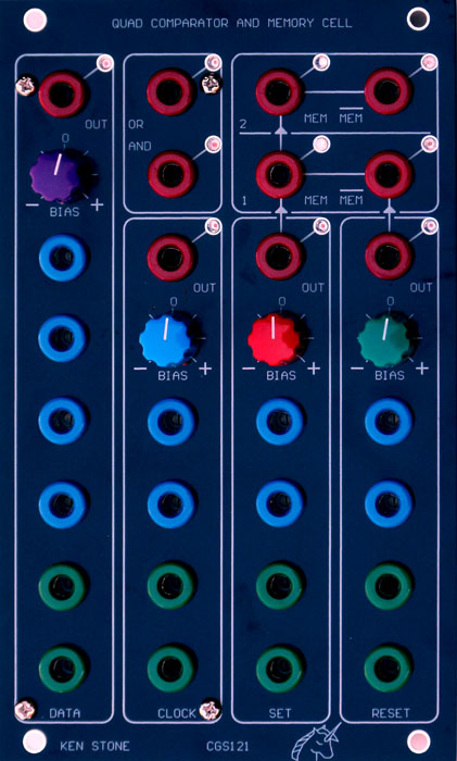
Quad Comparator and Memory Cell
Ā
Go here for a full description of the CGS121 and general build notes. The documentation on this page relates specifically to the build of the CGS121 using the CGS121 Panel.
The CGS121 Panel is made of 0.1" thick fiberglass, and has a ground plane on the front.
The rear includes some pads and traces to help with wiring and assembly.
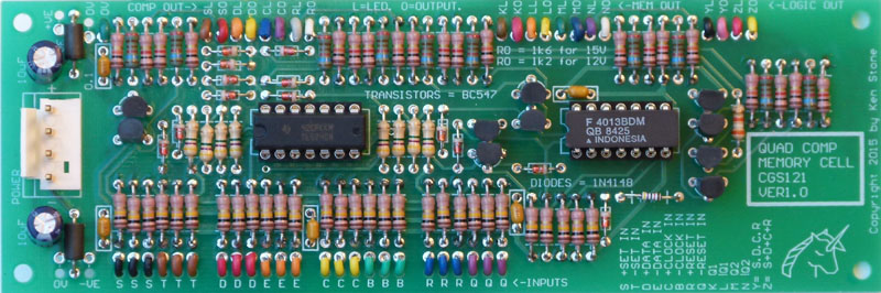
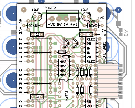
This shows the components that are installed on the PCB when building it for use with the PAN121 panel.
Note the zero ohm resistors are nothing more than nicely packaged wire links.
There are no components installed on the rear of the PCB.
3mm LEDs can be mounted directly on the panel, their own leads supporting them.
Form the leads as shown, so the leads are not stressed where they come out of the LED.
The LED cathodes go to the pads that are linked to the silver "bezel" around each LED hole.
Do not mistakenly fit LEDs to the mounting holes!
Do NOT drill out the LED holes to mount larger LEDS as doing so will sever their through-hole connection to the earth plane.
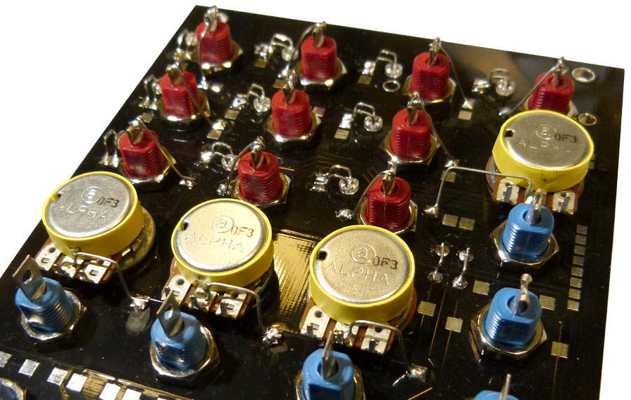
A piece of large diameter heat-shrink tubing or a piece of tape is wrapped around the body of each pot to prevent wires from shorting to their body.
Clippings from component leads are used to connect each jack to their appropriate pad.
Kken folded the tags down on the banana sockets to reduce the required board mounting height.
More wire clippings are used to connect the center (wiper) terminal of the pots to their corresponding pads, as shown. You may wish to insulate these, or use hookup wire.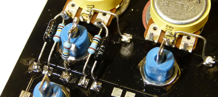
Resistors are mounted as shown, between the pots, jack and nearby pads.
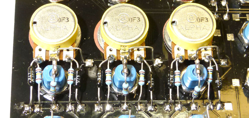
This is done for the three pots that are in a row.
Note that the wiring for the fourth pot is a little different.
The two 47k resistors go to the left, one having to pass over the pot. Insulate the lead of this resistor.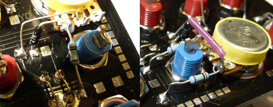
The left image shows the first 47k resistor soldered in.
The right image shows the second 47k, and its insulated lead.
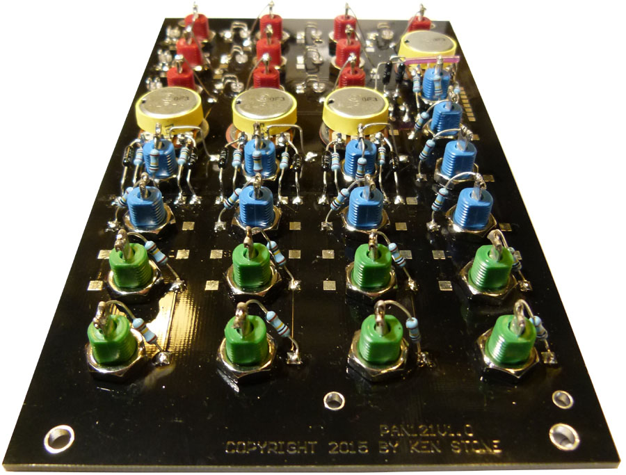
Blue jacks indicate an input that responds positively to an input, adding it to the tally for that channel.
A different color jack, in this case green, indicate that an input responds negatively, subtracting the input voltage from the tally for that channel.
As an individual may wish to use more or less of each type, the panel allows for some variation.
A 100k resistor from the jack to the pad on the left side of the jack results in a positive response, a 100k resistor from the jack to the pad on the right results in a negative response.
The bottom-most jacks only have a pad for a negative response, while the top most jacks only have one for a positive response.
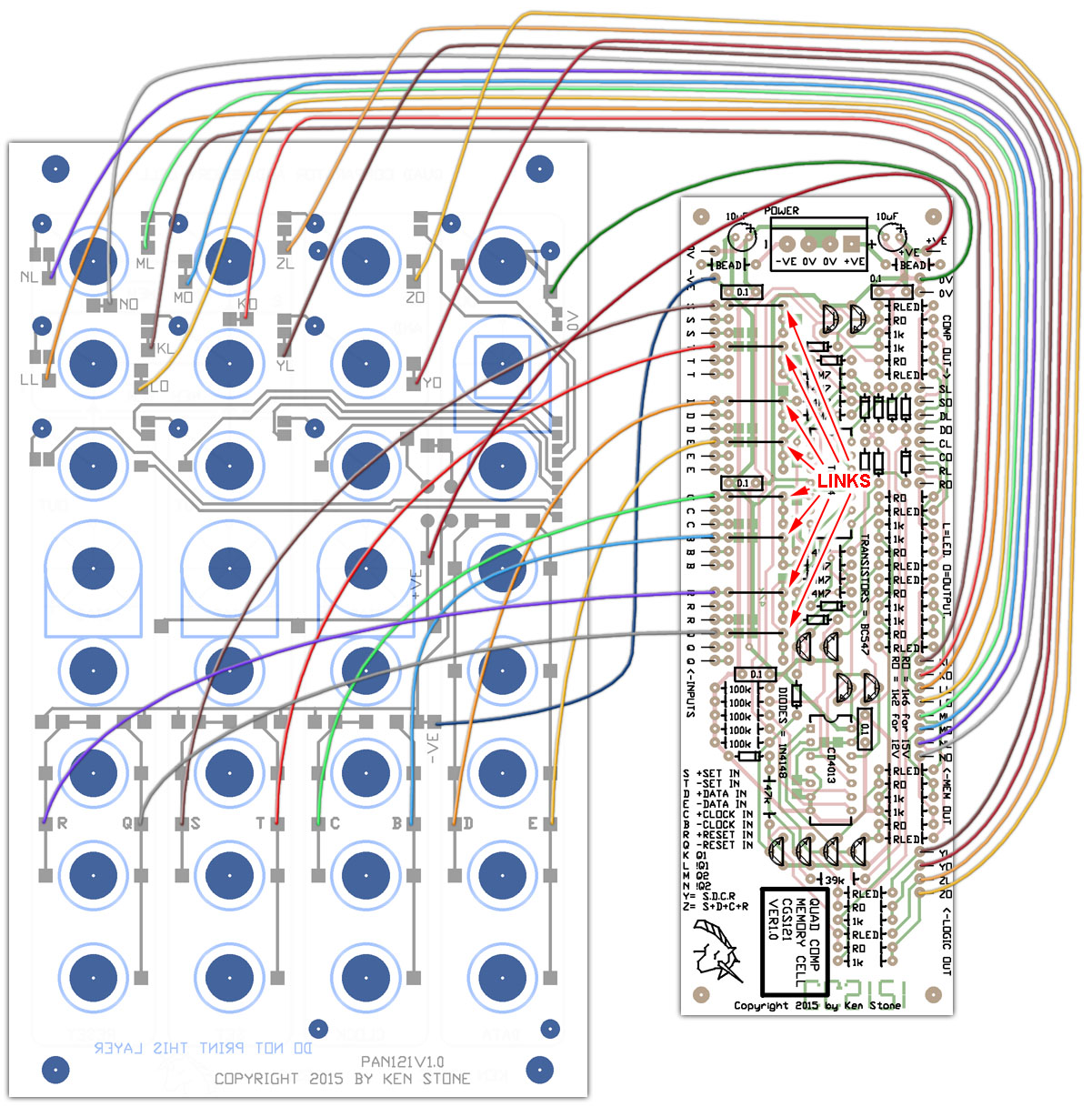
This diagram shows the hookup wire portion of the wiring for the CGS PCB panel PAN121V1.0
For the remaining eight connections, hookup wire could be used.
Alternatively a 0.1" spaced wiring strip would work.
Although the wiring strip is shown connecting to the top of the CGS121 PCB,
it may be easier to feed it through from the bottom and solder it on the top.
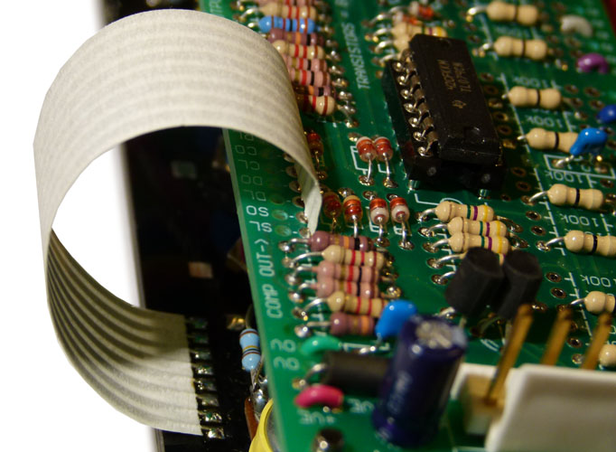
After soldering it on, the wiring strip needs to be folded away from the edge of the panel.
This particular strip is a little too long.
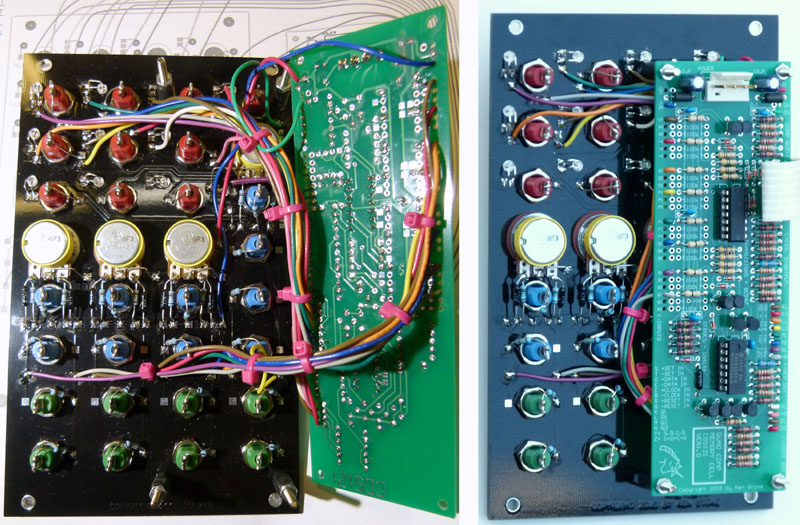
Completed wiring.
Article, art & design copyright 2013 by Ken Stone
|
