|
Wave Multiplier for music synthesizers. 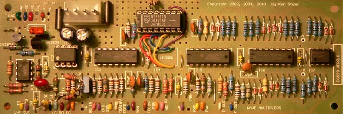
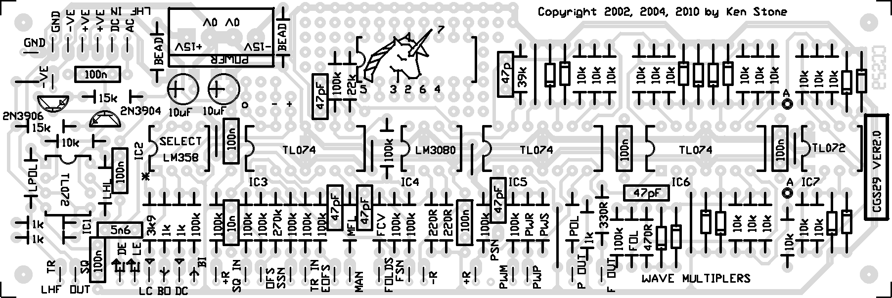
Photo of the VER2.0 PCB. Changes from V1.x: Two extra folding stages have been added to the main multiplier. The prototyping area has been modified to allow easy substitution of an LM13600/LM13700/NE5517N for the LM3080/CA3080, which is now obsolete. TL07x series chips have been substituted for the LM324. Resistors affecting levels have been marked. In addition to this, there are some suggested modifications to improve it further, though it will work without the modifications. Construction
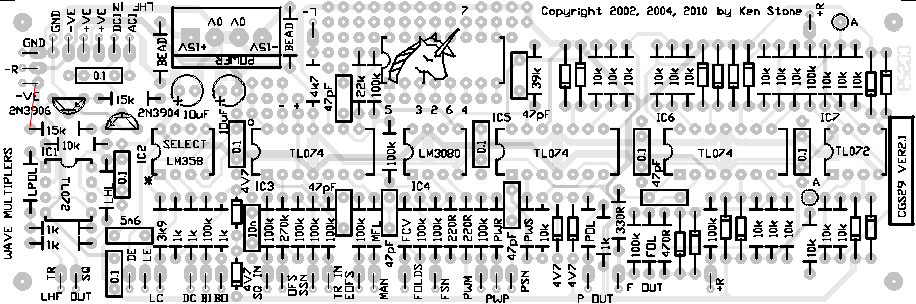
Modifications to the VER2.0 board These are shown on the circuit diagram in dark red. The addition of a 10k resistor and two 4.7 volt 400mw zener diodes wired back-to-back limits the total voltage going into the PWM comparator to a level that is less than the signal level of the multiplied waveform. This helps prevent signal drop out at the extremes of the PWM control range. It will not prevent drop-outs when the 'Folds' setting is at its lowest, or when the input signal is too weak to cause any wave folding to occur. This requires a track to be cut on the rear of the PCB. The addition of a 1k resistor and two 4.7 volt 400mw zener diodes wired back-to-back at the output of the Grinder limits the output waveform to roughly +/- 5 volts. Without these diodes, the output can easily reach the near-power rail voltages. These parts can be tacked on the PCB as shown in the photo, or they can be added between the PCB and the output jack. The 5n6 specified affects the frequency of the instability in the Grinder. Other values may prove more satisfying to your ear. On this occasion I substituted a 15n and used a 100k pot instead of the original 1M. Additional construction notes for the VER2.0 PCB: There are two pads marked DC. do not confuse them. One is the DC input for the Lockhart and is located near the text "LHF IN". The other is the wiper connection for the Grinder Drive pot and is also marked with a small triangle. Additional construction notes for the VER2.1 PCB: An error has been found on the VER2.1 PCB. In the Lockhard multiplier the end of the 15k resistor that is meant to connect to the -VE rail has somehow become isolated. A short link to the nearby -VE pad will correct the problem. At assembly time, this can be done by folding the resistor lead across to the adjoining pad and soldering it before trimming it. See the PCB image above for the location. It is marked in red. Resistor Designations:
The 100n AC input capacitor on the Lockhart should be at a polyester type such as greencap or MKT. The remaining six 100n can be ceramic monoblock decoupling capacitors. 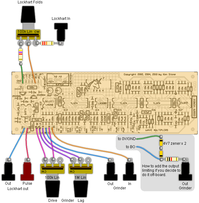
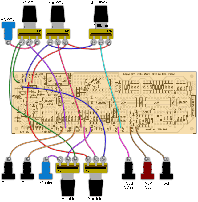
Wiring the VER 2.0 PCB version of the Grinder and Lockhart folder.
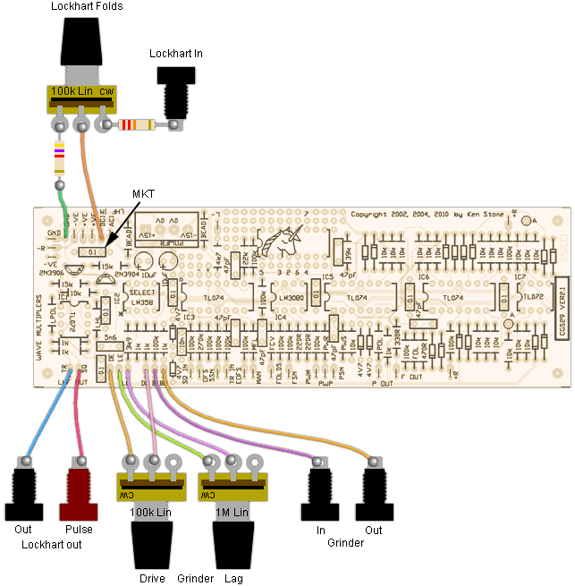
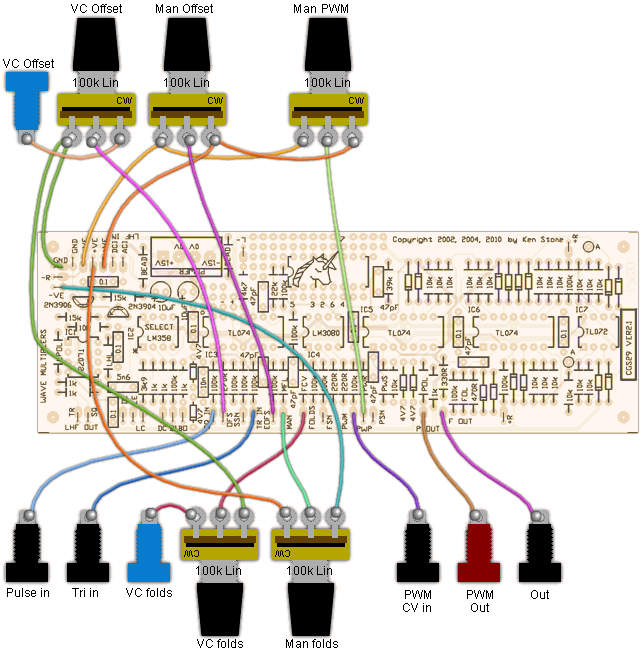
Wiring the VER 2.1 PCB version of the Grinder and Lockhart folder.
Article, art & design copyright 2002 by Ken Stone |