
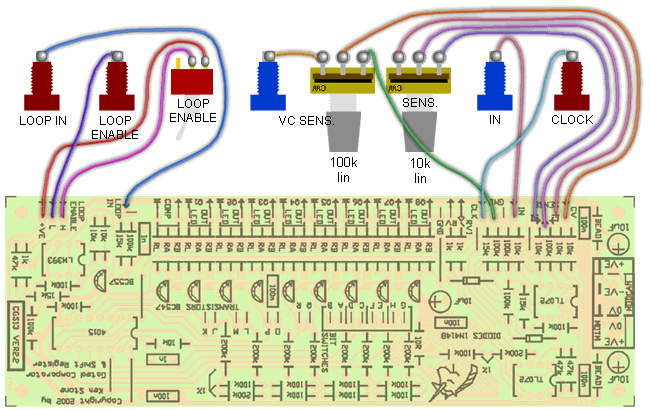
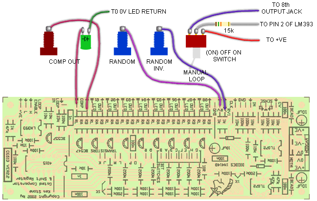
Gated Comparator The idea for this project came when Ken was listening to some music in which part of the background was jumping between octaves in a semi-random fashion. Feeding noise into a comparator was my immediate thought, but he soon realized this wasn't going achieve what he wanted. Ken needed to be able to control when these jumps could occur. As such, some form of memory element was required, into which the level could be clocked when required. Ken has used an 8 stage digital shift register as the memory element. Each clock pulse, the remembered level (logic 0 or logic 1) is moved into the next stage "bucket brigade" fashion, and the new value stored in the first memory cell. The result is a random level (on or off) at a predetermined time at the first output, plus time delayed versions of previous levels across the remaining outputs. As well as the 8 shifted gate outputs available, the raw comparator output is also available. The status of each of the outputs is displayed by a LED, making adjusting the unit so much easier. There is also a secondary voltage control input so the comparator break/reference point can be varied by an external control voltage. On top of all this, there is a D/A converted connected to the outputs of the shift register, with the last 4 bits capable of being switched in or out. This gives some great little melodies or sequences. They will depend largely on what is fed into the shift register, though due to the configuration will always have a certain flavor. There is an inverted output for this as well. When the resultant voltage is fed to a VCO, effects from subtle semi-random melodies to 70s sci-fi computer sounds can be generated. Version 2 adds a Loop input so that several gated comparators can be cascaded together, or its own output can be fed back into its input. Other digital sources could also be used. This new "digital" input is OR gated with the original "analog" input, so keep this in mind when patching. It is quite possible to rapidly set all stages in a loop to HIGH, in which case there will be no further activity on the outputs. Loop Enable has two inputs. The "H" input is for connection to a panel mounted switch to set your default preference. Connect this to one side of a SPST switch. The other side of this switch goes to +VE. The "L" input is for external control via a jack. This input will override the switch setting unless a high impedance output is being used to drive it. Most Synthesizer outputs are low impedance, so it should not be an issue. Note that it is active LOW. A positive gate on this input, or the switch being CLOSED results in the loop being disabled. Swap the connections to pins 5 and 6 of the LM393 if you wish it to work the other way around. How to use this module: Connect the input to a noise source, LFO, VCO or other signal source. Connect a LFO or similar clock signal from a sequencer, etc. to the clock input. Connect the shift register outputs as required to VCOs, VCFs or other clocked modules, and/or connect the CV (RV and RVI) outputs to a module that requires a CV input. The unit can also be used as a simple gate delay, where the delay is controlled by the frequency of the clock signal. The length of the resulting delayed gate signal would of course be a multiple of the clock period. A little on how it works:
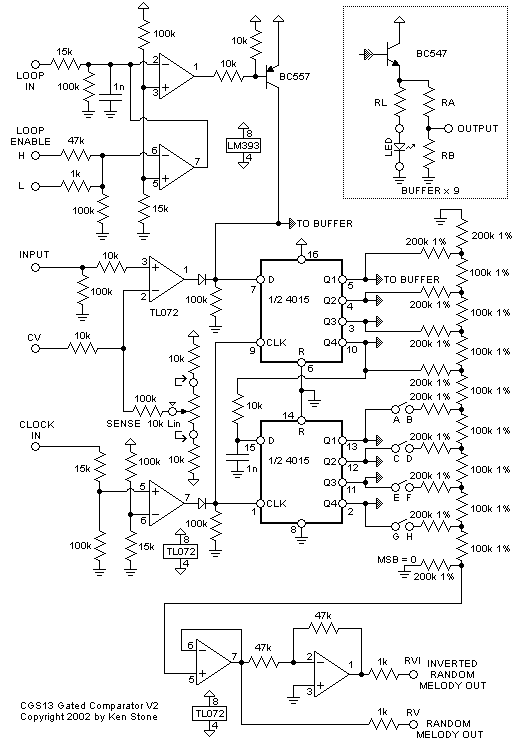
The schematic of the Gated Comparator. The circuit consists of two comparators, one with it's sensing point adjustable by a front panel knob an and external CV. This is for processing the input signal, and the other to square up the gate or clock signal and provide some isolation for the CMOS shift register (4015). Each of the digital outputs is buffered by a transistor/resistor buffer. The two shift registers in the 4015 are clocked from the same source. The fourth output of the first shift register needs to be slightly delayed to ensure reliable loading of the second shift register. The outputs of all of the shift register stages are also fed to D to A converter consisting of an R/2R resistor ladder and an op amp wired as a voltage follower. A second op amp provides an inverted output. Construction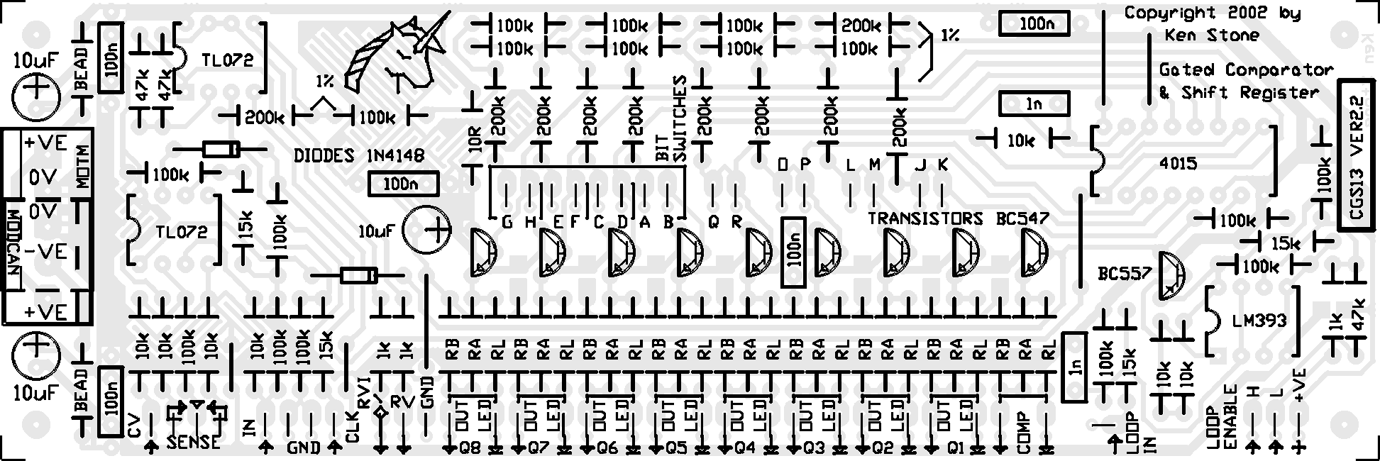
1206 SMT bypass capacitors have been used on the rear of the board. The are simply soldered between each pair of square/rectangle pads without holes. We recommend starting assembly by first fitting the RB resistors. Solder only the pad nearest the edge of the PCB and then trim all the legs leaving the unsoldered legs about 1mm long. Solder the right-hand pad of each of the SMD capacitors. Place the capacitors while heating the already-soldered pad. When all the capacitors have been installed, solder the left-hand pad/RB right-leg combinations. 
The LED resistors (RL) can be selected as needed. If you are using common LEDs, 1k to 2k2 would be appropriate. If you are using any of the super-bright modern LEDs for their unique colors, the resistors can be much higher, 10k to 33k for example, so that the LEDs don't dazzle you. Resistors RA and RB form the voltage divider that determines the gate output voltage. Use 1k for RB. When running off +/-15 volts use 1k8 for RA. When running off +/-12 volts, use RA = 1k5. Pad pairs A-B, C-D, E-F and G-H are to allow for optional switches to add the 5th through 8th bits to the random melody output. If these are left open, the melody will be limited to 16 notes. Optionally a header can be installed, allowing removable links to be used to set the desired number of bits semi-permanently. Pad pairs J-K, L-M, O-P, Q-R are so the same can be done to the first four bits, but unlike the ones above, these are pre-linked by PCB tracks. These tracks will need to be cut if adding switches for these bits. The tracks that are to be cut form a "V" between each pair of pads. 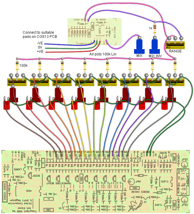
Notes:
CGS13 Tutorial By Nicholas Peck At 'Under The Big Tree'
Parts list Article, art & design copyright 2001 by Ken Stone |
