|
This module is an analog control voltage shift register, three stages in length. It duplicates the functionality of the Serge ASR, but goes about it in a very different way. It is great for producing "arabesque-like" sequences, trills etc., when used with VCOs. Of course it's use is not limited to VCOs only. Unlike ASRs produced using "bucket brigade" techniques, the CV outputs are constant from the beginning of the cycle to the end - there is no "charge period" in which a brief glide is heard. The CV input/output range of the ASR is approximately +/- 10V. How to use this module: Connect the CV input to a voltage source such as a keyboard or sequencer. Connect the three CV outputs to the three modules to be controlled. Connect the clock input to a LFO or other low frequency trigger source. To cascade the unit with others, connect the clock inputs to the same trigger source, and connect the third CV output of the first ASR to the CV input of the second ASR. Unlike the Serge ASR, there is no need to used delayed trigger pulses. A little on how it works: 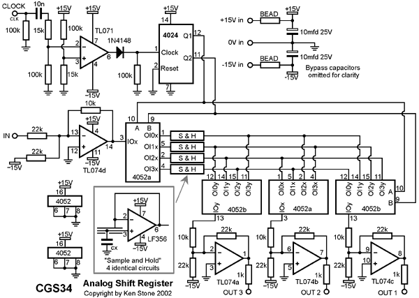
The schematic of the Analog Shift Register. The ASR is nothing more than a 4 stage analog memory. Each cell of this memory is a capacitor, followed by an LF356 buffer. Addressing each stage of this in turn is half of a 4052 4 pole analog switch. As each cell is addressed, it is forced to follow the incoming voltage. The cell remains connected to the incoming voltage for a full clock cycle, giving it ample time to reach the correct level. At the same time as this is happening, there are three other 4 pole analog switches that are pointing to each of the other three cells. The first of these points to the cell filled the previous clock cycle, the second to the cycle before than, and the third to the one before that. As such, once each cell is filled, it remains that way for 3 clock cycles, then is filled with a new voltage on the fourth. The other three cells are cycled in turn to the 1st, 2nd and 3rd outputs. The TL071 and 4024 form the clock pulse to address converter. The remaining circuitry is an input buffer and three output buffers designed to adapt the voltage to that suitable for switching by the 4052. The input range of the ASR itself is approximately +/- 10V. Construction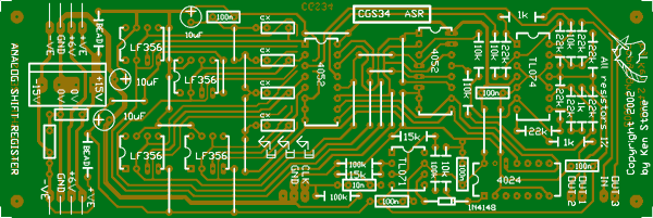
The component overlay. Connections can be determined from the circuit diagram. The capacitors specified as CX on the circuit board and diagram are the S&H capacitors and as such should be high quality low leakage sorts, such as polypropylene. The value of them will depend on the speed at which you intend to run the unit. The larger the capacitor, the lower the maximum speed at which it will run, but the longer it will be able to hold the voltage without drooping. 47n is probably the smallest that should be used, though drooping becomes quite noticeable at slow speeds. It may be possible to go as high as 470n for really slow operation, though this will somewhat limit the maximum speed (see the notes below). The 10k and 22k resistors in the input and output buffers should be matched 1% metal film for best results. Where do you get matched resistors? Buy a few more resistors than you need (maybe twice as many), and compare them with your multimeter! Generally, 1% will be close enough, but matching them will further reduce any errors. At the very least get the resistors from the same batch. Other FET input op-amps may work in place of the LF356. CA3140, CA3130 (wrong voltage) or TL071 would work though may introduce minor offset errors. CA3140 or CA3130 may reduce the rate of any "droop". CA3130 would require power supply modifications for the op-amps at the very least. Notes:
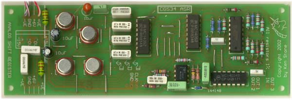
Parts list This is a guide only. Parts needed will vary with individual constructor's needs. Article, art & design copyright 2001 by Ken Stone
| ||||||||||||||||||||||||||||||||||||||||||||||||