This module is a "tribute" module, based on the awesome Steiner-Parker Synth VCF. Those who know Ken will know he is not a big VCF fan. Nonetheless, this VCF really appeals to him. Its sound is quite unlike the Moog ladder, has a lot of character. Resonance is a bit unusual in its behavior. Once it starts oscillating, the resonance pot needs to be backed off a fair way to get it to stop again. It can also be frequency dependent. How to use this module: Connect the CV input to a voltage source such as a keyboard, envelope generator or sequencer. Connect the output to a VCA or amplifier. Feed the signal to be filtered into the high-pass, band-pass or low-pass input. Unlike the original, this version allows signals to be fed into all inputs simultaneously. If the same signal is used in all inputs, the result is reminiscent of a phaser. The real fun starts when you feed different signals into each input, then you get a frequency based "interpolating scanner", where panning between different sound sources is possible, though also subject to the frequency at which they are running. I have never heard an effect like it before. A little on how it works:
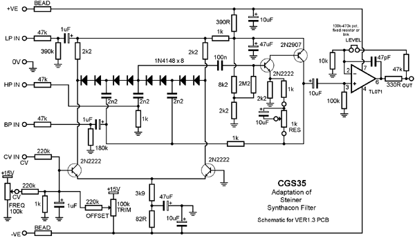
The schematic of the Ver1.3 Synthacon VCF PCBs. The circuit uses a standard, non-inverting amplifier configuration. The three modes (HP, BP, LP) are obtained by injecting the signal into three different points of the circuit. An increase in the gain of the amplifier increases the filter's Q. The Q remains almost constant as the filter is swept across the audio spectrum. In the circuit, diode strings are used as voltage controlled resistors. The differential-amplifier transistors apply the bias voltage to the parallel diode string RC networks in opposing phase. The opposing phases cancel the control voltage so that none appears at the output. The final pair of transistors form a non-inverting amplifier. The variable resistor adjusts the gain of this amplifier, and thus its Q. The final stage is a simple gain stage, as I found the original was too quiet for my needs. In the first version of the PCB, this stage was inverting, while on the Rev 1 PCBS, this stage is non-inverting. The LEVEL pads are to allow for a level pot to be installed. Use a pot with a value of 50k or 100k (going even higher if needed, e.g. 250k), depending on the overall gain required. Alternatively, a fixed resistor could be put here, or even a link, if the 47k in series with it is increased to compensate. Note that the level pot does NOT allow the output to be reduced to zero, as this is impossible to do with a variable resistor in the feedback circuit of a non-inverting buffer. It will adjust the gain from the default 5:1 up to 15:1 assuming a 100k pot is used, effectively allowing you vary the output from standard to three times that level. (Based on an article by Nyle Steiner from Electronic Design 25, Dec 6th, 1974.) Construction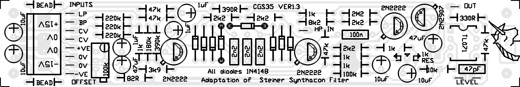
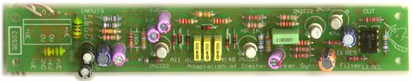
Construction Notes/modifications: Version 1.3 can be built as shown on the overlay of the PCB. No modifications are necessary for use with +/-15 volt supplies. For use with +/-12 volt supplies, the two diodes marked with rings around their pads on the overlay should be replaced with links.
A pair of pads is provided to allow the fitting of an output level pot. Something like 50k to 100k would be appropriate. The associated 47k resistor can be replaced with a link. If you do not require the level control, these pads MUST be linked together. Version 1.3 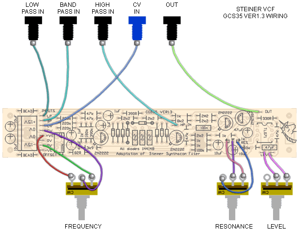
Notes:
Parts list This is a guide only. Parts needed will vary with individual constructor's needs. Article, art & design copyright 2001 by Ken Stone |