|
This is a new version of the Stomp Box Adapter. This time there is no provision for any jacks on the PCB. It can be used as an external input amplifier, a way to use effects pedals with synthesizer signal levels, or a way to use synthesizer modules with instruments such as electric guitars. A little on how it works:
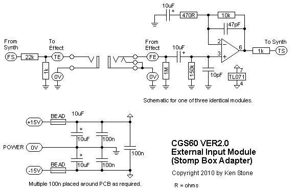
Modular synthesizers generally use much higher signal levels than are used in effects pedals, so directly connection the two will create two problems. First, the excessive signal will cause the input of the effects pedal to overload/distort. Second, the output from effects pedal is too weak to drive synthesizer modules without some amplification. To compensate for these problems, the signal from the synthesizer must be dropped to a fraction of what it was, while the output of the effects pedal must be amplified by the same amount to restore it to a level suitable for the synthesizer. I have chosen to use a ratio of 20 as this encompases the signal levels of many synths. If you know for certain that the ratio is too great, the ratio can be reduced to reduce the amplification of any effects pedal noise. For example, if an effects pedal works on a 1V p-p signal, and a synthesizer has a maximum output of 5V p-p, a ratio of 5 would be adequate. The preamplifier of the stomp box adapter is a basic non-inverting amplifier with an AC gain of 20, and suppression capacitors as needed. The input impedance is approximately 150k. The AC gain can be reduced if need by by increasing the value of the 470R resistor. For example, a 1k resistor in this position would give a gain of 10. The 1k resistor of the input divider would need to be increased to 2k2 to keep the drop and gain matched. Construction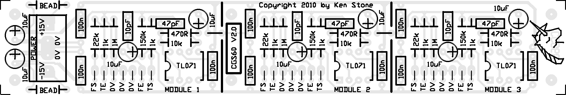
There are three identical "modules" on this board. Depending on your requirements, you may need only insert parts in one or two of them. Each is clearly segmented on the PCB. It would also be possible to separate this board into three sections, each with two mounting holes. Two would need off board 10uF decoupling capacitors and a power connector. There are pads provided on the rear of the circuit board for 1206 or 805 100n decoupling capacitors. You can install these or regular through hole capacitors. There is no need to install both types. Any single op-amp with industry standard pinouts can be substituted as needed.
To use the wire anchor holes:
Notes:
Parts list Parts needed may vary with individual constructor's needs. Article, art & design copyright 2003 by Ken Stone |