|
Gate Converter for music synthesizers. The purpose of the Gate Converter is to turn standard positive gate signals into negative to positive going gate signal. This is particularly handy when interfacing to other manufacturer's modules that require a zero crossing signal to operate. It can also be used to convert assorted LFO or VCO signals to square or rectangular waves, to extract some form of gate signal from an envelope and so on. A little on how it works:
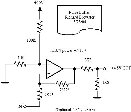
The schematic of the Gate Converter. This circuit is a basic comparator with a little hysteresis. It is set to detect input voltages above or below the reference voltage of approximately 1.4 volts. The output of the comparator is then reduced by the resistive divider to approximately + or - 5 volts, depending on whether the input voltage is above or below the reference voltage. There are 4 identical units on the PCB. Construction
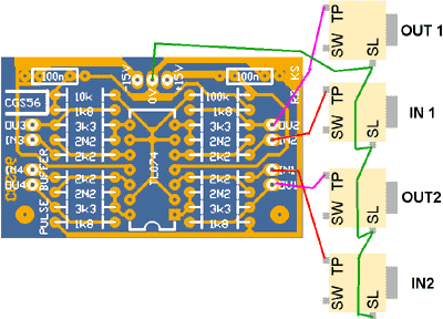
The component overlay of the first version of the board, including a wiring example.

The component overlay of the VER1.1 PCB. Wiring remains the same as the example shown above Click here for an enlarged printable version. This board can be integrated into a module as either an input processor or output processor, or wired up as a regular utility module. Notes:
Parts list
This is a guide only. Parts needed will vary with individual constructor's needs. Article, art & design copyright 2004 by Ken Stone |