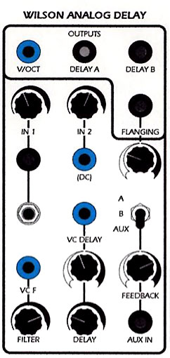
Serge Wilson Analog Delay
DISCONTINUED
The CGS208 WAD module is a recreation of the Serge Wilson Analog Delay module.

The schematic of the Wilson Analog Delay. Click for larger view
Construction

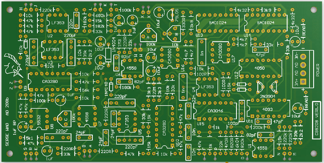
The component overlay for the VER1.0 PCB.
Click here for an enlarged, printable version. Print at 300dpi.
![]()
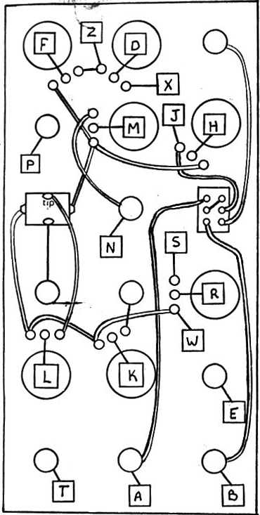
Connections to jacks can be established from the schematic diagram
Setup

Function blocks of the PCB.
There are two variants of the vintage WAD. Both use the same PCB. The only difference is the value of some resistors.
The following readings were taken from a working late model GENUINE WAD.
Very Important: before power is applied, turn Trimmer B fully clock-wise. Failure to do so before power-on may damage the 3080s.
Do not TURN this trim pot fully CCW, or past the halfway point!
The following tests are to be done without the Analog delay chips installed.
Despite the above, as I was taking readings from someone else's working WAD, my tests were performed WITH the SAD1024 still in their sockets. The test document also assumed the board was not connected to any panel controls, where here it very clearly is. The only real differences this makes is instead of injecting external voltages into some pads, you adjust the pots to set the voltages. Initially the pots are set to output 0 volts. For the Filter frequency, this means turning it fully CW. For the Delay pot, it means setting it to the center of its rotation.
VC clock tests
1) check for a square wave at 15000 Hz +/- 40% with a 0 to +12 Volt amplitude at pins 4 and 12 of the 4050. (The period of the wave may be anywhere from 50 through to 70 through to 100 microseconds). If you do not get a square wave +/- 10% duty cycle, then check the CA3046.

2) check for pulses about 1.5 microseconds long (at 15000 Hz) at pins 10 and 4 of the 4093.

This waveform will be at both pins.
If these tests fail, check components in the VC clock section of the PCB.
Input VCF tests
1) feed the square wave from pin 12 of the 4050 into pad L (the input). The output at pin 1 of U3 should be almost a sine wave of about 5 Volts peak to peak. Adjust trimmer A if there are flattened spots on the wave. (If test 1. fails and the sine is more or less than 2.5 Vp.p check resistors and caps in the input VCF section.)

Ignore the synch echo. The sine was around 2.5 volts as shown.
2) Input a variable voltage of 0 to -5 Volts at pad P and check that varying the voltage results in a smooth and undistorted attenuation of the sine wave.
If this test fails, first check resistors R57, R58 and R59 (47k, 22k and 1k) and the CA3046. Then check components of the input VCF section.
3) Connect a voltmeter to the output as above (pin 1 of U3).
Disconnect the VCF input and CV.
Measure the voltage. Input +12 into pad D.
Measure the voltage.
The difference in the two readings should be -0.190 volts +/- 10%.
If the readings are off, check the values of the resistors in the input VCF section.
The voltages here were 4.4 volts and 4.55 volts, a difference of 0.15 volts, well within the required window.
+6 volt regulator check
- Check for +6 volts +/- 7% at the junction of R23 and R24.
(This can be measured between the 0 volt power supply connection and pin 5 of U5).
Check these resistors and the polarity of C6 (10uF) if it is off.
Negative volt regulator check
- Check that the outside lead of the 79L05 is -5V +/- 10%. If not, check whether Trimmer B is fully clock-wise, as per the Analog Delay Testing section above.
- Also check the polarity of the associated electrolytic capacitors and the regulator itself. As the voltage specified here is pre-adjustment, it is of little consequence. The tested unit was set to -6.64 volts. Be aware that this is the trimmer that can blow up CA3080 according to what is written above.
Test of the dual S&H sections and the output low pass filters.
1) Take a 2000Hz sawtooth (0 to +5) straight from a VCO (e.g. the blue jack of a PCO) and feed it into pin 3 of U16 (CA3080). Use a 1k series resistor between the VCO and the chip to protect it. Check for a stepped replica of the saw at pin 1 of U4. (The bottom of the sawtooth wave will be flattened out.)

There are two waves superimposed on each other here. Both are set with the center line being 0 volts. Sync is being taken from the triangle wave (input). The stepped wave at P1 of U4 appears to be affected by some sort of jitter here, possibly via some feedback from the SAD1024 via another part of the circuit. Without the SAD1024s installed, the wave would probably be clearer. Note that P1 is sitting well above 0V, centered roughly around 4V
2) Now connect the scope to pad A and check for a rounded version of the saw. You may have to adjust Trimmer C to center the trace (around 0V). Repeat step 2 of the "Input VCF Test" above, but check for a progressive attenuation and filtering of the sawtooth wave at A.

Same oscilloscope settings as above. This is the "rounded" version of the saw, and a whole pile of echoes. Don't expect the echoes if you are testing with the SAD1024s out of circuit.
If a S&H doesn't work, check for the presence of the short 1.5 microsecond pulses at pins 10 and 4 of U11, and in much reduced form, near -12 volts, at pin 5 of each of U16 and U17. Check parts in the S&H area if these pulses are missing or incorrect.
If the low pass filters don't work, check construction and component values in the low pass VCF section.
Turn off the power and install the SAD1024 delay chips.
Feed a sine wave of about 200Hz (via a mixer) to input pad L. Monitor pin 12 of U13 and adjust Trimmer A until the (clipped?) sine wave is well centered (around 0V). Using the mixer, drop the amplitude of the sine wave until it is just barely clipping, and readjust Trimmer A for most symmetry.

This image shows the sine wave (input) and the frightful looking output of the SAD chip.
Note that the output of the SAD1024 is well above 0V.
The lower portions of the wave are around 0.7 volts while the upper portion is centered roughly around 3 volts.
Remember, these readings are being taken from an adjusted unit.
Now monitor pin 7 of U4. Adjust Trimmer B for the most symmetrical sine wave. As above, you may need to adjust the amplitude of the incoming signal to be able to successfully adjust this trimmer.

This is the signal at pin 7 of U4.
No tweaking was done to the input level or anything.
It is simply what the waveform of the previous signal looks like after going through the S&H.
If there is no signal at pin 7 of U4, monitor the outputs of the SAD1024 chips, one stage at a time, starting with pins 12 and 5 of U13, and pins 12 and 5 of U14. Also check the resistors in the analog delay section.
Final musical tests should be done with a short transient sound at a 2 per second repeat rate, with a 100Hz saw into a VCA. Feed CVs into the proper inputs, check ranges and proper filtering action, check the flanging output (pad E). If this doesn't work refer to the S&H, LP filter and output flanging sections.
Notes:
This module is designed for +/-12 volt operation.
Parts list:
This is a guide only. Parts needed may vary with individual constructor's needs.