|

Triple Bi-directional Switch This module is a variation on the 1973 Classic Serge Triple Bi-directional Router, and the 1975 Bi-directional Quad Switch modules.
Bi-directional Quad Switch. Construction 
If you are planning to use it with 6.3mm or 3.5mm jacks, the common of these jacks should be wired to 0V/GND as usual. Just solder the return wire to the (unused) center pins of the power connector. We would suggest powering the module for the first time without any chips in it and checking the voltage between the emitters of the two regulating transistors (BC547 and BC557). If this voltage is over 15 volts, you will need to change the values of the resistors in the voltage divider.

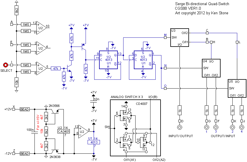
When building the Bi-directional Quad Switch, install all parts except for the 22k resistors. Wires need to be run from the pads marked M, N and O to one pad of each of the empty 22k resistor locations. See the photo above. You also need to link pads C to L and B to H complete the routing. In this configuration, the I input is the only one used. A positive gate or trigger signal will advance the switch to the next input/output.

As the gates are in series, some the protection resistors are not required, but were present on the original Serge version, effectively doubling the resistance of the switch. You can replace these extra resistors with links. On the prototype, I shorted out the extra resistors on the rear of the PCB as shown above. 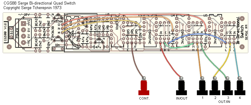
Set UpThere is no setup. Notes:
Parts list This is a guide only. Parts needed will vary with individual constructor's needs. Article, art & design copyright by Ken Stone |