|
3D Model |
Overlay |
Plan View |
Column 1 PCB |
|
|
|
Column 2 PCB |
|
|
|
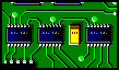
ES37 PCB |
|
|
|
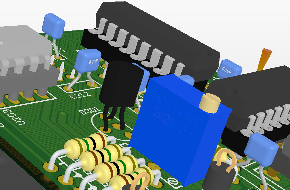
Constructors should refer to the Component Overlays along with,
the Bill of Materials for the current value of all components, and
the General Construction Notes for general PCB assembly guidelines.
- Assemble the 2x Switch Carrier Boards
- Assemble the 8x Jack Carrier Boards
- Fit all components to the boards except for the sub-assemblies
- Fit 1x switch sub-assembly and 4x jack sub-assemblies to the Column 1 board but do not solder
- Offer the assembly up to the front panel and secure using the supplied nuts
- Check that the PCB is parallel to the edge of the panel
- Solder the sub-assemblies in to place
- Repeat for the Column 2 board
- Mount the back board ensuring it is correctly aligned with the IDC headers
- Fit the jumper shunt on JP102 in the position marked ‘4’
Addendum
There is an error with the footprint for D301
- If fitting the LM336 you should cut off Pin 1 first and not solder that pin
- If fitting TL431 you should refer to this image for the correct orientation.

