Assemble the jack carrier board for J1 (3D Model)
-
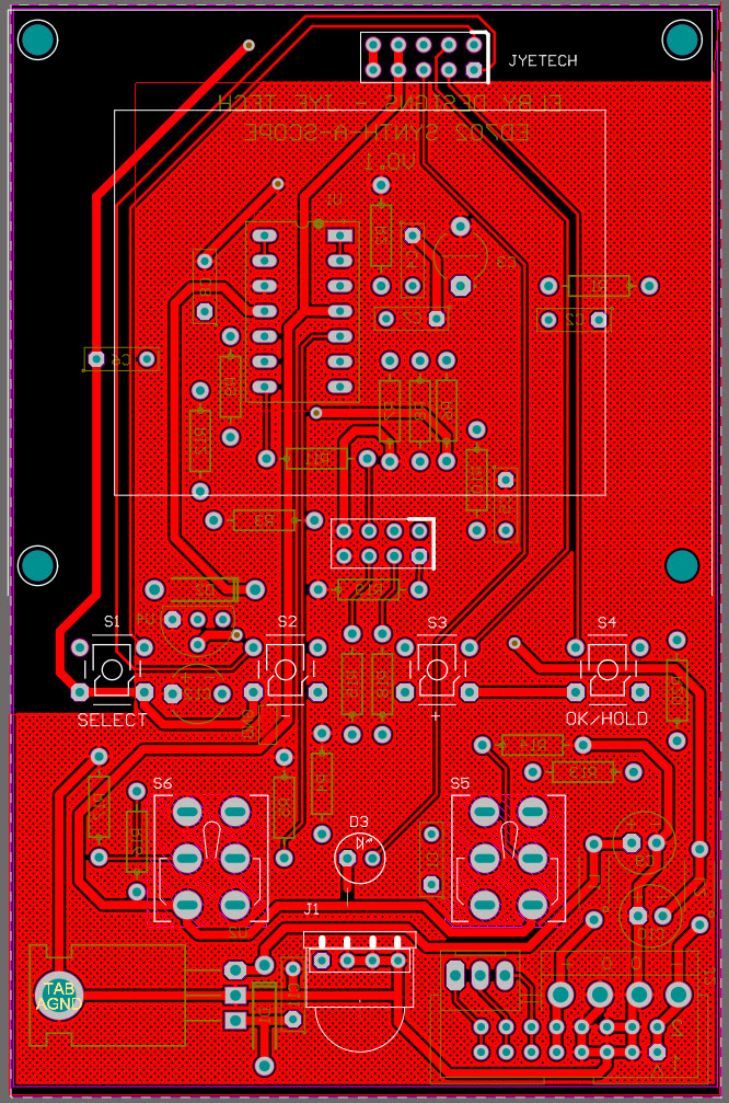
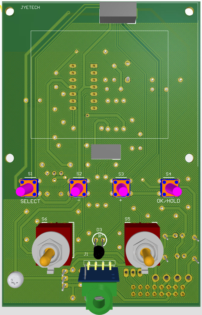
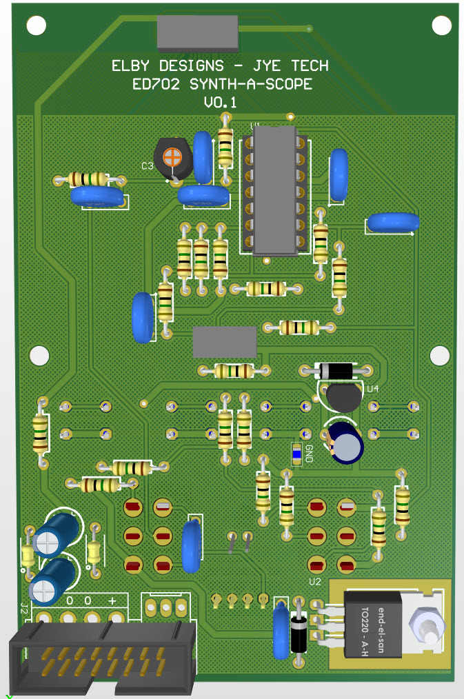
Populate the main board with all components except D3, J1, S1, S2, S3, S4, S5 and S6
-
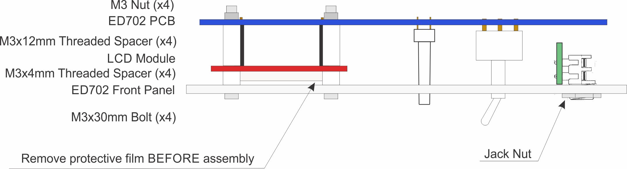
Remove the protective film from the LCD
-
Fit the 4x M3x30mm bolts to the front panel using the 4x M3x4mm spacers
-
Carefully slide the LCD on to the bolts and secure using the 4x M3x12mm spacers. Note the orientation by referring to the 2 headers
-
Fit the LED lens mount
-
Position all the remaining items on to the board but do not solder. Note that D3 needs to be mounted in reverse to that shown in the PCB footprint.
-
Carefully offer the board up to the front panel being careful when inserting the headers from the LCD module
-
With everything in position secure the main board to the front panel using the 4x M3 Nuts.
-
Finger tighten the nut on the jack J1
-
Solder all components in to place ensuring that the pushbutton switches are square to the board and move freely. Ensure that the LED D3 is firmly seated in the lens mount before soldering.
-
Finally, add a wire link to D3 as shown on the overlay and in the 3D Model

