|
Wave Multiplier for music synthesizers. 
Photo of the VER2.0 PCB. The idea for this project came from the fabled middle section of the Serge wave multipliers. At the time Ken designed this, he had never seen or heard one of these units, nor had he seen its schematic diagrams, but armed with descriptions and suppositions by various people who had seen them, and a couple of photos of CRO traces from the output of the module, he decided to design himself one. The result as displayed on the CRO is very close to those of the Serge, with the exception of the final fold, where, in Ken's design, the wave maintains more of its original shape. It can produce the most amazing, harmonically rich, filter-like sweeps. It took Ken weeks of experimentation before he came up with the final design. He tried various configurations (usually mixing the outputs of successive rectifiers) as suggested on websites devoted to the original, and while he did have success, there were elements of the designs that he felt were poor. It wasn't until he approached the problem from a different angle that he was happy with the result. The circuit he came up with he would describe as a "reflector", and is ingeniously simple. The day after he released the first version of this module, he was emailed the schematic of the Serge version, and apart from the value of the resistors, the "folder" was the same "reflector" he had designed. There were some other differences, such as in how Ken drove the VCA, and how the final fold was dealt with. Initially Ken decided to release a four-stage unit, having experimented with up to 7 stages. This version re-instates two of the folding stages. In addition to this multiplier, there are two more simple multipliers, one created by adding lag to the feedback path of an op-amp, the other being the "Nonselective Frequency Tripler" by R. Lockhart. Its functionality is not unlike Moog's single transistor sawtooth to triangle wave converter. It's intended purpose is to convert a signal into another of three times the frequency. To do this it expects a +/-1.2 volt triangle or sine wave, and outputs a +/-0.4 volt complex waveform. Unfortunately, due to the uneven spacing of the frequency multiplied waveform, it does not sound like it is a fifth above the incoming signal. This of course in of no particular concern in this application, as the purpose of this module is to create a complex harmonic structure from a simple input, not to triple the frequency. Input range of signals is +/- 5V. Greater signals will not damage it, but may cause distortion. How to use this module: For the primary multiplier, the "folder", connect the input to the triangle wave output of a VCO. Connect a LFO, envelope generator or even a DC voltage to the folds input. The result will be a harmonically rich signal at the "F out" output. A second input based on a lag circuit allows square waves and other hard-edged waveforms to be used as the signal source. There is also a "squared" output available, with "pwm" inputs to further vary the possibilities. To use the second multiplier, the "grinder", feed the input from the output of a VCO. Adjusting the "drive" and "lag" pots will give variation to the output signal. Obviously both multipliers can also be used to mangle control voltages, the outputs from LFOs etc. A little on how it works: The "grinder" is simply an inverting amplifier with a lag circuit in its feedback path. Depending on the time constant of the lag pot and its associated capacitor, the op-amp will take longer to settle. In trying to maintain the virtual ground at pin 2 of the first op-amp the output will overshoot, then as the virtual ground settles, then passes the optimal point, the output will again try to compensate, with the same results. The result is a "ringing" that is imposed on the input waveform around the points it changes direction. This introduces a lot of high frequency hash. The op-amp best suited to this circuit is the LM358. The characteristics of the grinder will differ significantly if another chip type is substituted. You may even find you need to try several LM358 variants and select the best. Construction:Notes on earlier versions are here
Where there was space on the PCB, Ken has provided extra pads so that various size capacitors can be fitted. There are several decoupling capacitors, none of which are shown on the schematic. There is provision on the rear of the PCB between the ic pins for an additional 5x 100n 1206 SMT decoupling capacitors. It is a good idea to insert a 100k resistor between the +Ve supply and the normalized connection on any CV jack you may chose to wire that way. This is because +Ve will momentarily be fed out of this jack when you plug something into it, due to the mechanical nature of the contacts. The pads marked R+ are there for this purpose. There is also an R- pad as well connected directly to the -Ve supply. The unused op-amp has been brought out to pads, though will require a couple of tracks to be cut if it is to be used. There is also a small prototyping area provided. If substituting a LM13600/LM13700/NE5517N for the LM3080/CA3080, you need to run wires from the 3080 pin locations to the corresponding numbered pad in the prototyping area. Two additional 220 ohm resistors are then soldered between Pins 14 and GND, and 13 and GND. The GND trace is immediately next to the provided pads. See the photo at the top of the page. As originally presented, the input level pot on the Lockhart wave folder allows the input to be taken right down to zero. If a 4k7 resistor is soldered between the CCW end of the pot and GND, the Lockhart will pass an essentially unmodified signal with the pot rotated to its CCW end, assuming a +/-5 volts or lower strength signal. Placing a 22k resistor between the CW end of the pot and the input jack limits the maximum amount of folding to +/- 5 volts. If a greater signal is fed to it, or if this upper resistor is omitted, the folded signal will continue to grow until it forces the op-amp into clipping, giving a signal strength near that of the power rails. The above resistor values were selected using a 100k pot that actually measured 110k, which is within tolerance. The resistor values may need tweaking depending on the pot chosen, and the signal strengths used in your synthesizer. (These resistors are marked with #1 on the schematic.) All version 2.x designs include 2 extra folding stages . If not required, then the TL072 at far right along with the 10K resistors and diodes above and below it should not be fitted and a wire link installed between the 2 points marked (A). The 4k7 used at the CCW end of the Lockhart Folds pot is now onboard on V2.2 PCBs and is accesible via the pad marked LO. Resistor Designations:
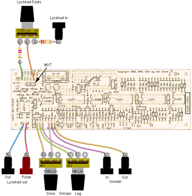
Wiring the VER 2.1 PCB version of the Grinder and Lockhart folder.
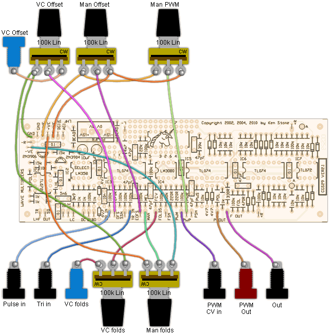
Wiring diagram for the BoCGS MARSH build of the CGS29 Wave Multiplier Notes:
Parts list Article, art & design copyright 2002 by Ken Stone |

