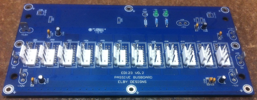
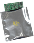
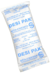
Being double-sided means that the PCB has tracks on both the TOP and BOTTOM layers of the PCB. Where required, these tracks 'join' each other using a VIA which comprises 2 pads in corresponding positions on both the TOP and BOTTOM layer which are electrically connected by a hole through the board and which is then made electrically conductive by electroplating. These VIA's do NOT require the builder to apply solder to them - in general these will be 'tented' and so will not have any exposed copper. The PCB's use a RoHS compliant lead-free HASL surface finish. This has a good shelf-life and provides a good wetting surface for soldering. Although it is quite possible to use lead solder, better results are achieved using lead-free solder. HASL boards are not suited for fine-pitch surface-mount devices. A silk-screen is used on all boards to identify the location of each component. Being double-sided also means that it is possible to place components on both sides of the board. When components are to be mounted on the BOTTOM layer, their silk-screen will be printed on the BOTTOM layer i.e. ALWAYS mount the components on the side that their silkscreen is on. PCB Storage Many people are aware of the dangers ElectroStatic Discharge (ESD) can pose on a Printed Circuit Board (PCB). A standard bare PCB (meaning that it has no semiconductor components installed) should not be susceptible to ESD damage. However, as soon as you populate it with electronic (semiconductor) devices, it becomes susceptible according to each of the individual component’s susceptibility. The Problem With Moisture Moisture, on the other hand, may be a new issue to you. Surface Mounted Devices (SMDs), for example, absorb moisture and then during solder re-flow operations, the rapid rise in temperature causes the moisture to expand and the delaminating of internal package interfaces, also known as “pop corning.” The result is either a circuit board assembly that will fail testing or can prematurely fail in the field. Moisture from air diffuses inside the plastic body & collects in spaces between body & circuit, Similar problems can occur with the PCB itself. Moisture can be absorbed in to the PCB material and when exposed to excessive heat such as from a soldering iron, can vapourise causing delamination of both the PCB layers and copper tracks. If you have PCBs that have not been stored properly or have been stored for an extended period of time, you should consider oven drying them. PCBs should be separated and, preferably, stood on their sides in a rack so that all surfaces are exposed and placed in a cold oven (NOT a microwave oven). The oven should then be turned on with a setting of around 120°C for 2-4 hours. Once dried, PCBs should be soldered within 24 hours. Storing PCBs ALL PCBs should be stored in an air-tight bag (1) along with desiccant packs (2).
|


© Copyright 2000. All rights reserved. Revised: December 9, 2023