|
3D Model |
Overlay |
Plan View |
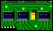
Column 1 & Column 2 PCB |
|
|
|
Column 3 PCB |
|
|
|
ASM317 PCB |
|
|
|
Constructors should refer to the Component Overlays along with,
the Bill of Materials for the current value of all components, and
the General Construction Notes for general PCB assembly guidelines.
- Assemble the 2x Jack Carrier boards
- Fit all components to the boards except for the 4x Jack Carrier sub-assemblies. Please refer to the notes below regarding the ‘Offset Circuits’ and ‘SEM Modification’ to decide if the associated components will be fitted or not
- Locate the 2x Jack Carrier sub-assemblies on to the Column 1 PCB but do not solder
- Offer up to the front panel and secure using the supplied nuts and washers
- Solder the 2x Jack Carrier sub-assemblies in to place
- Repeat steps (3) to (5) for Column 2
- Offer up the Column 3 assembly and secure using the supplied nuts
- Mount the ASM317 assembly ensuring correct alignment of the IDC connectors
SEM Modification
Additional parts (R128, R129, R130, D101 and D102) are included in your kit to allow you to add a feedback stage in the Q control circuitry. This modification was added by Gene Stopp in his ASM-1 design. For an original ENS-76 build, simply omit these components.
CV Rejection
P101 and P102 are included to allow CV rejection adjustment to the 2x OTA’s. In most cases this calibration is not needed and the trimpots and their associated resistors R106 and R111, can be omitted. If you prefer to fit them ‘just in case’ then the trimpots should initially be set to their mid-position