-
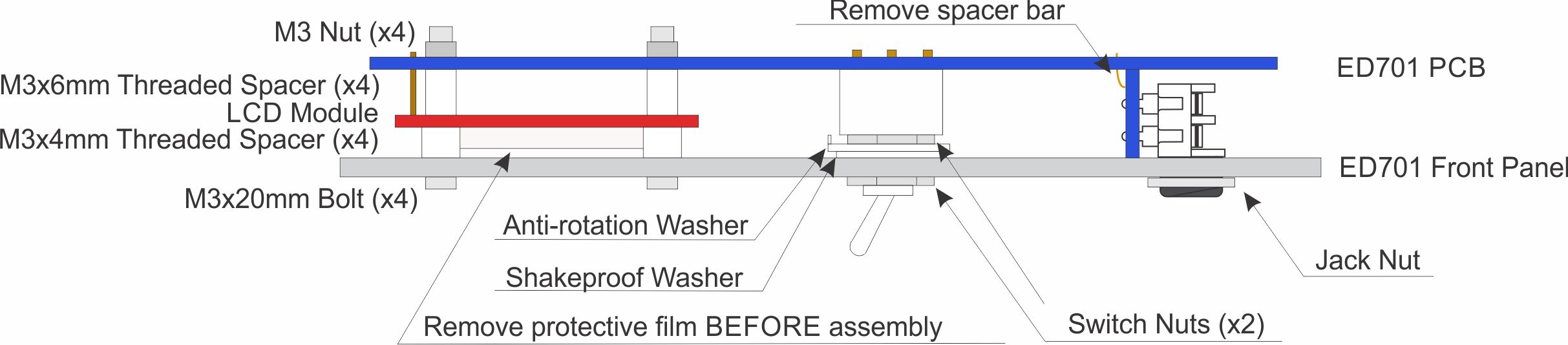
Assemble the 1x Jack Carrier PCB (3D Model)
-
Populate the main board with all components except J101, S101, S102, P101, S301, S302 and LCD1
-
Remove the protective film from the LCD.
-
Fit the 4x M3x20mm bolts to the front panel using the 4x M3x4mm spacers.
-
Carefully slide the LCD on to the bolts and secure using the 4x M3x6mm bolts. Make sure the PCB header is at the top of the module
-
Position all the remaining items on to the board but do not solder.
-
The 2 switches S101 and S102 should each have 1x nut, an anti-rotation washer and a shakeproof washer placed on them before mounting to the panel.
-
Carefully offer the board up to the front panel being careful when inserting the header from the LCD module.
-
With everything in position secure the main board to the front panel using the 4x M3 Nuts.
-
Finger tighten nuts on the switches S101 and S102 and the jack J101.
-
Solder all components in to place ensuring that the pot shaft remains central to the front panel hole while being soldered
-
Similarly, check the operation of the 2x pushbutton switches before soldering